

҈ SEM – Scanning Electron Microscope
Working Principle:
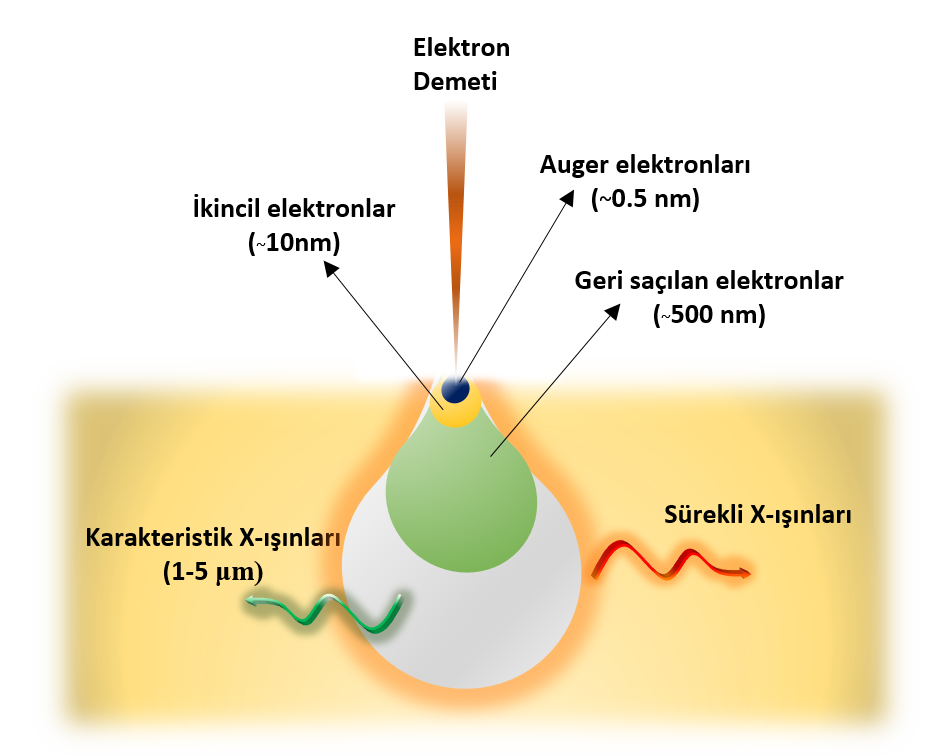
In SEM, high-energy electrons interact with the sample to generate electron and photon signals. Electrons scattered at different angles are collected by the detector and images are obtained as a result of processing the collected signals with the microscope software. Secondary electrons, material topography, and backscattered electrons provide information about atomic composition based on atomic number and contrast. In addition, the distribution of elements is mapped with point, linear or regional qualitative and quantitative analysis with the EDS detector.
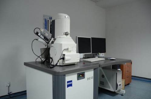
Scanning electron microscopy (SEM), designed within the framework of electro-optical principles, is a system that allows high-energy electrons to interact with the material and take an image from the sample surface. The ZEISS brand EVO 40 model SEM device within the body of the Anakara University Institute of Nuclear Sciences enables the imaging of the examined materials in micro and nano dimensions and the determination of the elemental compositions of the material with Energy Dispersive X-ray spectrometry (EDS)..
Samples examined in SEM:
Conductive samples
Coated insulator samples
Powder samples
Thin films
Biological samples
Polymers
Viewing Modes:
Secondary electron imaging (SE)
Backscattered electron imaging (BSE)
Low vacuum secondary electron imaging (VPSE)
Energy Dispersive X-ray detector (EDS)
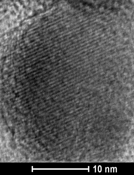
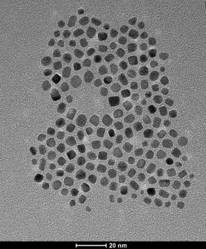
҈ Transmission Electron Microscope
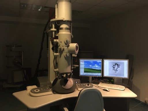
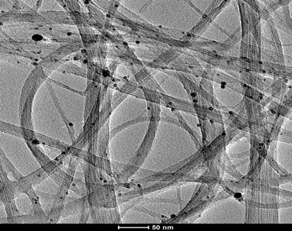
Transmission electron microscopy (TEM) are high-resolution systems that can process images by passing through the material or by diffraction as a result of the interaction of very high-energy electrons with a very thin material (<100 nm). Electrons passing through the material and undergoing diffraction give information about both atomic structure and material defects. Ankara University Institute of Nuclear Sciences has FEI brand G2 S Twin 200 kV RTEM.
Sample preparation:
Suspension forms are obtained by dispersing powder samples into suitable solutions by ultrasonic bath. The mixture is left to dry by dropping ~ 10μl on suitable coated grids with the help of a micropipette.
Samples examined in TEM:
Nanoparticle
Carbon nanotube
Nanoplate
Nanofiber
Polymer materials
Nanosponge
Bacteriophage
Polymeric-RNA